
Edited by Editor-in-Chief, The Indus Pulse 17 Sept 2026, 11:46 AM 3 min readtech
India Opens Semicon 2026 in New Delhi with 600 Exhibitors and 12 Approved Projects
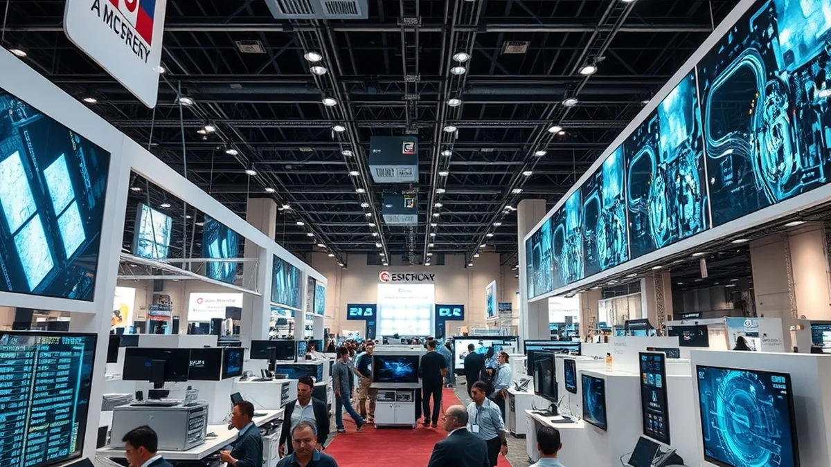
Prime Minister Narendra Modi inaugurated the fifth edition of SEMICON India 2026 at the Yashobhoomi Convention Centre in New Delhi on September 17, bringing together over 600 exhibitors and delegations from more than 50 countries. The three-day conference, scheduled to run through September 19 under the theme of silicon-to-systems ecosystem building, highlights the national push to establish a domestic semiconductor manufacturing and design base.
The opening event follows the Union government rollout of Semicon 2.0, an expanded framework backed by an outlay of ₹1.27 lakh crore aimed at growing domestic design capabilities and localized ancillary supply chains. Organised by the India Semiconductor Mission, the Ministry of Electronics and Information Technology, and SEMI, the exhibition floor spans roughly 15,000 square metres and features six country pavilions alongside twelve state government booths, though the released materials did not detail the specific states operating those pavilions.
Industrial Growth and Project Milestone Reviews
Ministry of Electronics and Information Technology officials confirmed that the Union government has approved 12 semiconductor projects under the broader Semicon India Programme. Three units cleared during the initial phase have already commenced commercial production. Major domestic conglomerates and global memory manufacturers, including the Tata Group, Murugappa Group, and Micron Technology, have advanced packaging, assembly, or fabrication timelines across various Indian states.
The event features more than 150 speakers and representatives from prominent international and domestic enterprises such as ASML, Applied Materials, Micron, Infineon, Lam Research, and Tata Electronics. Ahead of the formal opening, Prime Minister Modi chaired a roundtable discussion with executives from leading chip firms to review execution timelines, skilling initiatives, and infrastructure readiness.
Value Chain Integration and Design Focus
A primary feature of the 2026 exhibition is the complete production journey showcase, designed to highlight raw materials, equipment, advanced packaging, and finished systems. Unlike earlier initiatives that focused primarily on legacy manufacturing, the current policy framework places heavy emphasis on building domestic intellectual property and fabless semiconductor companies.
Semicon 2.0 broadens eligibility criteria for commercial chip-design entities, allowing companies owned and controlled by Overseas Citizens of India to participate provided they maintain headquarters and active technical manpower within the country. Eligible firms receive subsidized access to expensive electronic design automation tools and multi-project wafer services.
Talent Development and Skilling Targets
With workforce expansion treated as a distinct pillar under the updated policy framework, the administration is scaling up training infrastructure across technical institutions. Government data shows that electronic design automation tools have already been extended to more than 400 academic institutions and 105 startups, with 24 startups receiving direct backing under the Design Linked Incentive scheme.
Authorities report that student teams from tier-II and tier-III cities have successfully designed more than 250 chips. Building on an earlier milestone that trained 85,000 engineers over four years, the Ministry aims to develop an additional one lakh semiconductor engineers and generate up to 60,000 direct jobs as fabrication and packaging facilities scale operations toward commercial output.
Next Implementation Steps
The three-day exhibition continues through September 19 with parallel technical tracks covering display industry advancements, six dedicated country roundtables to secure joint ventures, and a forum focused on women leadership in microelectronics. Capital expenditure support tiers under Semicon 2.0 offer up to 40% backing for silicon wafer fabs and up to 35% for compound semiconductor and advanced packaging units, with support remaining open for ongoing project applications.
The Indus Pulse is committed to accuracy and transparency.