
India OSAT Push Faces Chip Testing Infrastructure Risks
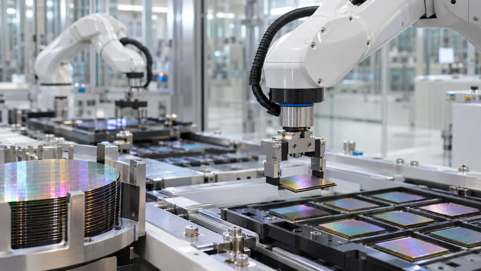
India's ambitious initiative to scale up domestic semiconductor assembly and outsourced packaging operations faces potential operational bottlenecks due to underdeveloped chip testing infrastructure. According to an analytical report from DIGITIMES in Bengaluru, the country's packaging capacity risks outpacing local testing facilities. Industry analysts warn that a shortfall in domestic testing capability could increase manufacturing costs and prolong reliance on overseas test facilities. As global chipmakers establish outsourced semiconductor assembly and test facilities across India, testing infrastructure remains a key link in the supply chain. Ensuring integrated testing alongside advanced packaging is critical to achieving comprehensive domestic self-reliance in commercial chip production.
India Packaging Push and Domestic Testing Bottlenecks
Concurrently, international semiconductor expansions highlight broader industrial challenges tied to infrastructure coordination, workforce demand, and manufacturing efficiency. In an interview with EE Times Asia during SEMICON West 2026, SEMI Americas president Joe Stockunas discussed global semiconductor dynamics. According to Stockunas, government commitments of $39 billion and private investments of $800 billion are driving unprecedented capacity additions in the United States. He highlighted that semiconductor manufacturing yields at advanced fabrication plants in Arizona have achieved operational equivalence to established facilities in Taiwan. However, converting capital investments into productive operational capacity requires seamless supply chain coordination and accelerated permitting procedures. The administration cleared a Gujarat testing facility proposed by Kaynes Semicon during September 2024 backed by the national semiconductor initiative, according to P&S Intelligence.
Global Fab Investments, Permitting Efficiency and Supply Coordination
He observed that semiconductor manufacturing is too complex for any single nation to provide all necessary capabilities, underscoring the necessity of global suppliers. For international equipment manufacturers, materials suppliers, and engineering firms, technical competence and innovative capability remain the paramount criteria. Workforce availability represents another acute operational constraint, with intense competition for engineering talent spanning tech giants and semiconductor foundries. Stockunas highlighted the recruitment of former military personnel and expanded science, technology, engineering, and mathematics education to alleviate technical labor shortages.
Workforce Constraints, Advanced 3D Packaging and AI-Driven Silicon Demand
Looking toward future architectures, the semiconductor industry expects artificial intelligence to drive exponential growth across generative, inference, and physical AI workloads. Within manufacturing environments, digital twins and AI optimization tools are improving fab energy productivity, which has expanded 10,000-fold over three decades. Future technological advancements are shifting beyond traditional planar transistor scaling toward three-dimensional chip stacking, advanced packaging, and optical photonics. According to Stockunas, SEMICON West will relocate to Phoenix, Arizona, in spring 2027, where over 60,000 industry jobs are projected. Global industry cooperation remains essential as emerging hubs in India and expanding ecosystems abroad navigate packaging, testing, and fabrication bottlenecks. In October 2025, Kaynes Semicon shipped India's first commercially packaged multi-chip module with 17-die intelligent power modules from its Sanand facility to US-based Alpha & Omega Semiconductor, according to P&S Intelligence.