
Andhra Gets First Chip Plant, Offers 80% Fab Capital Support
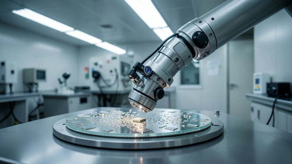
Andhra Pradesh is set to establish its first semiconductor plant near Visakhapatnam with a proposed investment of Rs 2,387.81 crore, while separately amending its Semiconductor and Display Fab Policy 4.0 to offer up to 80% combined capital support, according to The Hindu and Business Standard.
Visakhapatnam OSAT Facility
Advanced System In Package Technologies Private Limited is building the Outsourced Semiconductor Assembly and Test (OSAT) unit in Visakhapatnam district's Anandapuram mandal at Tarluvada village, The Hindu reported. Approved by the Ministry of Electronics and Information Technology under the India Semiconductor Mission (ISM) on August 20, 2025, it is the first ISM-sanctioned project to be grounded in Andhra Pradesh, according to The Hindu. ASIP's Andhra Pradesh semiconductor unit has an annual capacity of 96 million units under a technology tie-up with South Korea's APACT Co. Ltd, according to Press Information Bureau. ASIP Technologies stated that its Tarluvada OSAT facility will also create 1,600 indirect jobs. Through notification S.O. 6148(E) dated November 10, 2026, the Ministry of Commerce and Industry designated 12.14 hectares in Tarluvada and Gidizala villages as an SEZ and Inland Container Depot under the Customs Act for ASIP Technologies, according to ETGovernment. ASIP Technologies CEO Venkata Simhadri stated in August 2026 that the company aims to begin with wire-bond and flip-chip BGA packaging and have 2.5D packaging technology in production at Visakhapatnam by 2030 at the earliest.
The two-phase plant is projected to generate 1,000 direct jobs, starting with Rs 542.19 crore and 200 jobs in Phase I, followed by Rs 1,845.61 crore and 800 jobs in Phase II, The Hindu reported. After the State Council of Ministers cleared the proposal on February 24, 2026, formal orders from the IT, E&C Department on February 27, 2026 designated it a "special case", according to The Hindu.
That order directs APIIC (Andhra Pradesh Industrial Infrastructure Corporation) to allot 30 acres at Tarluvada at Rs 1 per acre and develop external infrastructure, while the State extends special incentives of up to 40% of the project cost alongside the Government of India's 50% grant, The Hindu reported.
Amended Semiconductor Policy 4.0
Separately, the State government amended its Semiconductor and Display Fab Policy 4.0 through G.O.Ms.No.87 dated November 16, 2026 to align with ISM Semicon 2.0, according to Communications Today. The State will match 100% of the Centre's capital support, giving silicon fabs 80% combined capital support (40% Centre and 40% State), compound semiconductor, photonics, sensor, discrete, display fabs, and advanced packaging 70%, and legacy packaging 50%, Business Standard reported. On November 6, 2026, Union Minister Ashwini Vaishnaw launched the Semicon 2.0 Web Application Portal, according to India Semiconductor Mission.
Andhra Pradesh compared its 80% silicon fab support against lower combined incentives in Gujarat (56%), Madhya Pradesh (60%), Uttar Pradesh (60%), Tamil Nadu (65%), and Odisha (65%), according to Business Standard. "Andhra Pradesh wants to be the place where India builds its chips, from design to fab to packaging," Minister for HRD, IT and Electronics Nara Lokesh said, according to Business Standard.
For chip design, startups can receive up to Rs 22.5 crore in combined seed funding, including Rs 7.5 crore from the State, and a 13.5% deployment-linked incentive capped at Rs 45 crore per application and Rs 180 crore per company, Business Standard reported. Machines and materials projects receive 48% combined capital support (18% State plus 30% Centre), R&D and talent projects get 25% State support capped at 75% combined, overall state incentives cannot exceed 50% of eligible fixed capital investment, and all-source support is capped at 90%, according to Business Standard.
The State also plans a 5,000-acre AP Semiconductor Park at Tirupati run by a public-private company, the AP Semiconductor Growth and Innovation Council as a single investor contact, the AP Semiconductor Research and Innovation Centre starting at IIT Tirupati with photonics first, and the AP Semiconductor Training and Capacity Building Centre offering a Rs 10,000 per trainee monthly subsidy for six months, Business Standard reported. Mega projects of Rs 1,000 crore to Rs 5,000 crore and ultra-mega projects above Rs 5,000 crore can receive customised packages from the State Investment Promotion Board, while non-Semicon 2.0 projects qualify for a Rs 3 per unit power subsidy for five years under the five-year policy, according to Business Standard.
Sources & Citations
- The Hindu
- Communications Today
- Business Standard
- Economic Times
- India Semiconductor MissionPrimary / official
- Economic Times
- Press Information BureauPrimary / official
- Press Information BureauPrimary / official